All Hardware Types Interview Questions
Digital Design/RTL
Topics
Overview
RTL Design involves designing and integrating digital logic modules for chips and IP blocks.
Successful interviews require both technical knowledge and strong behavioral preparation.
Behavioral Preparation
Critical for success. Be ready to discuss past projects with specific, measurable details.
"Improved circuit speed by 25%" is far more compelling than "worked hard on the project."
Prepare to explain:
- • Architecture decisions and tradeoffs
- • Performance improvements and optimization strategies
- • Debugging approaches and problem-solving
- • Design verification methods
Verilog/System Verilog
- Undoubtedly, Verilog and SystemVerilog are essential languages to master. You don't need to be an expert, but you must understand common syntax blocking/non-blocking, always, initial, the three types of fork-join, synthesizable statements, and frequently tested modules like sequence detectors and edge detectors. More challenging ones include FIFO and round robin. System Verilog focuses on OOP aspects; I wasn't asked about it much this time, but it's frequently tested.
- Be able to discuss and quickly implement the following structures:
- • Simple Counter
- • State Machine
- • FIFOs (synchronous and asynchronous)
- • You should know the minimum depth of asynchronous FIFOs.
- • Also, you need a reasonable test plan for FIFOs.
- • Full/empty detection for circular FIFOs (pointer comparison vs counter methods)
- • Arbiters (round-robin, priority, etc.)
Digital Design Fundamentals
- Logic design basics: universal gates, MUX implementations
- Counter design
- Basic multipliers and adders
- State Machines (major topic):
- • Draw state diagrams for scenarios
- • Mealy vs Moore models - critical to master both
- • Convert diagrams to Verilog - practice templates for quick implementation
- • Binary vs one-hot encoding tradeoffs
Computer Architecture - (See Computer Architecture section)
- OS Fundamentals (Important)
- Cache (Important)
- Memory hierarchy
- 5-stage pipeline basics
- Out of order execution
- Branch Prediction
- Parallelism
Static Timing Analysis
- Definitions: setup time, hold time, clock insertion delay, variation
- Analyze Flop-Logic-Flop configurations:
- • Detect violations
- • Fix violations
- Time borrowing, metastability, MTBF
- Logic optimization:
- • Karnaugh maps, mux/decoder implementations
- • Glitches in combinational circuits - identify and resolve (hazard covers)
Programming & Scripting - (More details in DV section)
- C/C++:
- • Leetcode (View the most common DV questions at the bottom of the page)
- • How to write Makefile
- • Typical C++ knowledge based questions - OOP concepts, Classes
- • Given a snippet of code, be able to explain the logic.
- Scripting: Python
Protocols & Interfaces
- Understand the working principles of some SOC communication protocols, such as AXI, PCIe, I2C, UART, and SPI; these are frequently asked in interviews. Having a project you're particularly proud of is a great asset. When interviewers ask me to describe a project on my resume, I always choose that one because it's something my teammates and I worked on from the very beginning. We had a clear understanding of all the design and optimization details, and the final result was quite good, so I felt confident when discussing it.
Things you should cover:
- Valid-Ready handshaking (ubiquitous)
- AXI protocols if applicable
- Backpressure mechanisms (valid-ready, valid-afull, valid-credit)
Clock Domain Crossing (CDC)
- CDC techniques and synchronization methods
- How to synchronize 1 bit or multiple bits, grey code and potential problems
- Know how to calculate the minimum clock cycle or propagation delay of a given circuit
- Handling data crossing clock domains safely, some cases to consider:
- • Slower clock domain to faster clock domain
- • Faster clock domain to slower clock domain
- • Crossing between clock domains with lots of data
- • ... and know what happens if you don't handle it properly for these cases
- Synchronizers (2-flop, multi-flop)
- Handshaking protocols for CDC
FPGA-Specific Roles
- FPGA vs ASIC differences
- Optimized RTL for FPGA architectures (register abundance, DSP blocks)
RTL Design Fundamentals
wire and reg?Select the boolean equation that matches the following truth table:
| A | B | C | O |
|---|---|---|---|
| 0 | 0 | 0 | 1 |
| 0 | 0 | 1 | 0 |
| 0 | 1 | 0 | 1 |
| 0 | 1 | 1 | 0 |
| 1 | 0 | 0 | 0 |
| 1 | 0 | 1 | 1 |
| 1 | 1 | 0 | 0 |
| 1 | 1 | 1 | 1 |
- a)
(A xor B) and C - b)
A or (B and C) - c)
A xnor C - d)
B - e)
B and C - f)
A xor (B xor C)
If we used lookup tables (LUTs) with 4 inputs and 1 output to implement the LogicModule module below, how many lookup tables would be used?
What is the value of A & B at various times of simulation - 0 time_unit, 1 time_unit, 2 time_unit, 3 time_unit?
a=1, b=0, c=0 just before a rising clock edge, compute the final values of a, b, c after one clock for each snippet.Variant A – Non-blocking (<=)
a, b, c for Variant A and Variant B? (Show your steps by drawing a waveform or a small timing table.)always @(posedge clk) begin : pipeline
Q1 = in;
Q2 = Q1;
Q3 = Q2;
end💡 Click to reveal solution
Q1→Q2→Q3 in the same cycle. That doesn’t model pipeline flops (each stage should capture theprevious cycle’s value). Use non-blocking (<=) oralways_ff to model sequential behavior.RTL Coding Challenges
💡 Click to reveal solution
wr_en and rd_en are 1 in the same cycle?Implement a frame filter module that accepts input frames and forwards only good ones. The module should:
• Drop any frame with an error on any beat
• Drop frames with invalid start/end sequence
• Apply backpressure when FIFO/buffer is almost full
• Handle frames of variable length (1 beat to many beats)
• Ensure no partial frames are sent to the output
out_valid is asserted, output (latest_value, second_largest_so_far). Example stream: 1, 4, 5, 2, 3 → on first out_valid: latest=3, second_largest=4; on next out_valid: latest=2, second_largest=4. Duplicates count as the second-largest value. State assumptions (bit width, signed/unsigned, duplicate handling, reset behavior, latency)💡 Click to reveal solution
Every new input:
1. Push input into S1
2.
If input >= L1
Push L1 into S2
Push input into L1
else if input >= S2
Push input into S2
else
Push head S2 into S2
Clk_50Mhz – 50 MHz input clockReset_n – Active-low resetData_in_1..4 – four 16-bit data inputsData_out – 16-bit data outputWE – write enable for selected inputAddress – 2-bit selects which input to writeWe get an async event.
If ≥1 event: Count as 1 event
If 0 event: Miss.
Requirements:
- • Create system to raise error flag if we have 2 misses every 40 cycles
- • Modify to raise error flag for 2 misses in any 40 cycle window
a[15:0]+b[15:0] → s[15:0]; now requirea[7:0]+b[7:0] → s[7:0] and a[15:8]+b[15:8] → s[15:8] using that single adder. State assumptions (single-cycle vs multi-cycle/time-multiplexed, latency allowed, carry behavior).💡 Click to reveal solution
H(z) = Y(z)/X(z) = (1 + 2z-1 + z-2) / (1 − 1.5z-1 + 1.5z-2).
Specify structure (Direct Form I/II or transposed), fixed-point widths/quantization, overflow/saturation behavior, latency, and reset strategy.
💡 Click to reveal solution
FIFO Design
a) A system has a 100MHz write clock. The write logic performs 16 write operations within 80 clock cycles. The write pattern is flexible (can be burst or random). What is the minimum read frequency required to ensure that the write operations are never backpressured?
b) After finding the frequency, what is the minimum depth that this FIFO should have?
💡 Click to reveal solution
💡 Click to reveal solution
Burst I assume is 100 cycles and not bits. So 1800 bits written in 100 cycles while read drains (36/60 x 20/18) x 1800 = 1200 bits in the same time. 600 bits to buffer, divides by 20 for 30 entries.
If you want to add sync delay to this, assuming read starts after a delay, can have 3-4 more entries.
💡 Click to reveal solution
Architecture:
• Register the output (out_r).
• Keep an odd-number counter starting at 3 and increment by 2.
• On each step: out_r ← out_r + odd_count.
Adders required: 2 (one for the odd counter, one for out_r + odd_count).
RAM Design
How would you implement malloc() and free() in hardware (Verilog)?
You are designing a pipelined memory access block with the following input request interface:
•
valid: Indicates a request is present when its value is 1.•
addr: Specifies the memory address.•
read: A control signal; 1 for a read request, 0 for a write request.•
count: For write operations, this is the data to be written. For read operations, it should be ignored.The block connects to a single-port memory with:
• Read latency = 3 cycles: Data becomes available 3 cycles after a read request is accepted.
• Write latency = 3 cycles: The written data becomes visible to subsequent reads 3 cycles after a write request is accepted.
Operational assumptions:
• One request per cycle can be accepted (no backpressure).
• Requests may target the same address (
addr) in consecutive or nearby cycles.Implement the block such that:
1. Writes update memory with the
count value.2. Reads return the value stored at
addr as of the correct architectural ordering of requests (i.e., as if processed in arrival order).The output interface is:
•
out_valid•
out_data (This output is only meaningful for read operations).• Reads must produce exactly one
out_valid pulse with the correct data.Task: Describe the microarchitecture and provide enough detail that someone could implement it (pipelines, queues, comparators, control rules).
AXI-Stream 5x5 Line-Buffer Design
You are given an AXI-Stream video-style input:
•
s_axis_tdata - 8-bit pixel•
s_axis_tvalid•
s_axis_tready•
s_axis_tlast - end of line•
s_axis_tuser - start of frameResolution is fixed (e.g., 1920 pixels per line), 1 pixel per cycle.
Question: Design an RTL block that outputs a 5x5 pixel window every cycle using only line buffers (BRAM-based).
Output is also AXI-Stream:
•
m_axis_tdata - 25 pixels (5x5 window)•
m_axis_tvalid•
m_axis_tready•
m_axis_tuser - aligned to center pixel•
m_axis_tlast - aligned to center pixelWhat you must explain in your answer:
1. How many line buffers are required and why?
2. How horizontal pixel delays are created for each line.
3. How the module knows when the 5x5 window is "valid."
4. How
tuser and tlast must be delayed to align with the center of the 5x5 window.5. What happens at borders (first 2 rows/columns).
6. How you keep the AXI-Stream protocol compliant (
tvalid/tready).Low-Power & Power Intent (UPF)
💡 Click to reveal solution
Why:
1) Area & Power: Latches are smaller/lower power than flops; savings multiply across thousands of ICGs.
2) Timing slack: A negative latch is transparent when clk=0, giving the enable nearly a full cycle to meet timing. A negedge FF gives ~½ cycle, tighter and riskier.
3) Glitch-free gating: In a standard ICG, latch output is ANDed with clk. While clk=0, the AND output stays low so enable changes can’t glitch the gated clock; latch closes at clk↑ and propagates a stable enable.
Using a posedge FF risks races at the AND; a negedge FF offers no benefit over the latch but costs more area/power.
Advanced RTL Topics
Things to think about:
a) What interfaces would you use? How many?
b) How would you arbitrate between requests?
c) How many ports does memory have?
d) What other blocks your memory controller should have?
Design Verification
Topics
Overview
Design Verification involves writing tests for digital logic modules to ensure comprehensive coverage of all use cases and corner conditions.
Behavioral Preparation
Same concepts as RTL Design roles (see RTL section)
Verilog/System Verilog
You won't need to write SV for complex structures such as round robin arbiters, but you will be asked how to test them (e.g. how would you test a FIFO?).
See RTL section for more details.
Digital Design Fundamentals
Same concepts as RTL Design roles (see RTL section)
Computer Architecture
Same concepts as RTL Design roles (see RTL section)
Static Timing Analysis
Same concepts as RTL Design roles (see RTL section)
Clock Domain Crossing (CDC)
Same concepts as RTL Design roles (see RTL section)
Programming & Scripting
Enhanced requirements compared to RTL roles (see RTL section):
Object-Oriented Programming
- You should at least be proficient in one of C++ or Python, with a preference for C++. Then, do some LeetCode easy-level problems. If you really can't solve them, just look at the answers, but after looking at them, you should definitely write some code and run it yourself.
- I recommend some recursive and string problems, such as Fibonacci sequence and palindrome detection, although my reason for recommending them is simply that I've seen others encounter these problems on the forum.
- I only did about a dozen problems in total, so the key isn't how many problems you do, but rather understanding the usage of data structures and algorithms. We're not computer science, so we don't need to know so much.
- There is a list of all the most common leetcode questions for DV at the bottom of the page.
- C++ is good for SystemVerilog's OOP foundation
- Sometimes skipped in interviews, but valuable knowledge regardless
- Understand and code examples for OOP principles:
- • Classes, Objects, Abstraction, Encapsulation
- • Inheritance and Polymorphism (frequently tested - identifying object class relationships)
Scripting
- Automation scripting is also very important; for example, printing specific information from a file. I didn't know how to do that, so I felt quite helpless when asked about it.
- Python works well for entry-level interviews these days since CocoTB is becoming more and more popular.
- Common pattern: parsing and processing large text files
- • Practice file I/O operations
- • Basic string parsing
UVM
This is only for non-internship roles, unless you have experience with UVM at work before.
UVM Cookbook should be enough preparation for the interview. Chipverify is also good. UVM mostly asks sequence/driver questions.
You need a good understanding of the verification architecture, including how generators, drivers, monitors, and scoreboards work. Ideally, you should be able to do some simple projects yourself. UVM is supposedly Big Plus, but it's normal not to know it; it's not a negative factor.
What to Expect
DV interviews are particularly challenging because you're expected to be a strong designer as well. Prepare all RTL Design content thoroughly.
- Verilog design questions often appear (typically simpler than RTL-focused roles)
- Strong digital design fundamentals separate good candidates from great ones
- For experienced candidates:
- • With prior DV experience (including internships), expect deep dives into UVM and advanced verification concepts
- • RTL Design questions may be minimal or skipped entirely in these cases
Verification Methodologies & Strategies
UVM
💡 Click to reveal solution
UVM factory is used to register classes and instances with a factory. e.g. uvm_object_utils, uvm_component_utils, type_id::create("<inst_name>"). New() is the default constructor of SV.
💡 Click to reveal solution
Class override and instance override
💡 Click to reveal solution
run_test()
💡 Click to reveal solution
Pointer to the actual interface. uvm_config_db is used for setting and getting the pointer to the actual interface.
💡 Click to reveal solution
A sequencer that contains pointers to all other sequencers.
💡 Click to reveal solution
Most commonly used phases: build_phase(), connect_phase(), run_phase(), check_phase(). Check_phase can be used to check size of queues and flag an error if queue is expected to be empty at the end of a simulation. Run_phase() is a task while the rest are funcitons.
💡 Click to reveal solution
Testbench Components:
- Test
- Environment
- Scoreboard
- Predictor (optional)
- Agent(s)
- Monitor
- Sequencer
- Driver
- Virtual sequencer (optional)
- Coverage monitor (applicable if you do class based coverage collection)
- Other models necessary in your testbench (e.g., memory model, etc.)
Sequencer-Driver Handshake: The sequencer generates transactions and sends them to the driver through a TLM (Transaction Level Modeling) port. The driver requests transactions from the sequencer using get_next_item() or try_next_item(), and when done processing, calls item_done() to signal completion back to the sequencer.
💡 Click to reveal solution
Note: All but 2 of my screening interviews had this question. The interviewers mainly want to see whether or not you understand some key components of a monitor. Interviewers don't care about syntax.
SystemVerilog Testbench & Constraints
💡 Click to reveal solution
In other words, within the 32-bit value, there should be no sequence of 5 contiguous bits that are all set or all unset.
💡 Click to reveal solution
Explanation:
foreach (arr[i])- Iterates through each bit positionif (i <= 27)- Only check positions where we can fit 5 consecutive bits (positions 0-27)!(&arr[i+:5])- Ensures no 5 consecutive 1's (AND of 5 bits is 0)!(&(~arr[i+:5]))- Ensures no 5 consecutive 0's (AND of inverted 5 bits is 0)
Write SystemVerilog constraints to divide the elements of this queue into three new queues (q1, q2, and q3) such that:
- • Every element from the original queue appears in exactly one of the three new queues
- • All three queues together contain unique elements (no duplicates)
- • Each queue must have at least one element
- • You cannot use
post_randomize()to perform the split - it must be handled entirely within the constraint block
How would you approach this problem?
💡 Click to reveal solution
Explanation:
idx[15]- Array of shuffled indices to randomize element assignmentunique {idx}- Ensures all indices are unique (no duplicates)q1.size() + q2.size() + q3.size() == array.size()- Ensures all elements are distributedq1.size() > 0; q2.size() > 0; q3.size() > 0- Each queue has at least one element- The
assign_to_queueconstraint uses the shuffled indices to assign elements from the original array to the three queues
- • Exactly three elements are identical (i.e., one value appears three times)
- • All the remaining seven elements are unique
How would you implement this constraint?
💡 Click to reveal solution
Explanation:
val[10]- Array of 10 random unsigned bytesval3- The value that appears exactly 3 timesval[i] < 10- Constrains each element to be less than 10val[i] != val3 -> val.sum() with (int'(item==val[i])) == 1- If an element is not equal to val3, it must appear exactly onceval.sum() with (int'(item==val3)) == 3- val3 must appear exactly 3 times in the array
💡 Click to reveal solution
What are some use cases for wait fork and disable fork? How would one kill thread_2() after fork-join_any below finishes and then continue waiting for remaining threads to finish? You can make changes to the code below if needed.
Upcasting vs downcasting. What does "virtual" keyword do in SystemVerilog?
What will be the output of the following code block? Update the code block to print the lines below (in any order).
• thread id: 0
• thread id: 1
• thread id: 2
bit [7:0] input_array[]; int unsigned input_count; rand bit [7:0] output_queues[$][]; constraint test_c { output_queues.size() == input_count; }STA/Static Timing Analysis
systemverilog logic [63:0] c; logic [63:0] b; logic [63:0] a; assign c = a + b;- How does this synthesize?
- How will you optimize this design for timing?
- Change the RTL based on your new optimized design.
- Given the following unit area values for each of the gates in this design:
- Full Adder: 8 unit area
- Half Adder: 5 unit area
- XOR gate: 3 unit area
- AND gate: 1 unit area
- What will be the area for the old design?
- What will be the area for the optimized design?
- What will be the critical timing path of the old design?
- What will be the critical timing path of the optimized design?
Clock Domain Crossing (CDC)
- a) Recirculation-mux with a synchronized ready
- b) FSM-based synchronized req/ack (any frequency ratio, but limited throughput)
- c) Asynchronous FIFO (higher throughput, extra hardware)
Bus Interconnect Design (AXI/APB/Custom)
Why might an AXI memory-mapped burst transaction hang if the target AXI-MM slave is reset during an active transaction, and what measures can be taken to prevent this situation?
What does the following constraint indicate to the tool about the logic driven by clocks clk_a, clk_b, and clk_c?
Embedded Systems/Firmware
System Design & Architecture
- Block diagram of tasks and functionality
- RTOS vs no RTOS decision
- Data protection and passing mechanisms
- Reliable periodic data transfer while another task sends data at a non-deterministic rate
Protocols & Interconnects
Embedded Coding Challenges
pow(x, y) for integers with fast exponentiation. Handle negative y and overflow.Questions:
- How would you design the system to count the number of people who have entered using this signal?
- How would you keep track of the current state of the turnstile within the microcontroller?
- Suppose a person stops halfway through the turnstile, keeping the signal high until they move again. How would you handle this condition to ensure the count remains accurate?
- Delimiters: any non-alphanumeric character (treat consecutive delimiters as one split)
- Do not use strtok/strtok_r/strsep. Use pointer arithmetic or your own scanning
- Time: O(n)
Function to implement (one of):
Output format (exact):
Examples:
Function signature:
Input parameters:
const struct OrderBatch *order_batch: a pointer to an `OrderBatch` struct to be serialized.const size_t out_max_length: the number of bytes allocated in `out`. Do not put serialized data outside of the pre-allocated buffer.
Output parameters:
uint8_t *out: the pre-allocated buffer to store the serialized `OrderBatch` data.
Return:
FuncStatus_t: the status of serialization effort. See enum descriptions below.
Provided non-standard type definitions:
Structures:
FuncStatus_t:
Background:
The serialized output data will have the following format:
- Note 1: Assume the host is little-endian.
- Note 2: You may receive an `OrderBatch` where `order_count` is less than 1.
- Note 3: Payload Len is the number of bytes in the serialized input including the first 10 bytes (i.e., `0xFACE` and Payload Len).
Serialized Layout:
Examples:
Example 1
Inputs:
Output (hex dump):
Returns:
Function signature:
Description of function parameters:
Input parameters:
uint32_t numBytes: The number of bytes in the array named `data`.uint8_t data[]: The byte stream of data to search.
Return:
-1: Returned if the given pattern (`0xFE6B2840`) is not found.-2: Returned if the input data is `NULL` or the size of the `data` is insufficient to find the pattern (`0xFE6B2840`).- Otherwise: the pattern is found. Return the starting bit position of the pattern (`0xFE6B2840`).
Background:
Two C library functions, htonl() and ntohl(), are provided for endian conversion:
uint32_t htonl(uint32_t hostlong);(host to network order)uint32_t ntohl(uint32_t netlong);(network to host order)
Note: Network byte order is big-endian, host byte order is little-endian.
Examples:
Example 1 - Byte Aligned:
Inputs:
Returns:
Example 2 - Non-byte Aligned:
This is the same as Example 1, left-shifted by 1 bit.
Inputs:
Returns:
Starter Code:
Function signature:
Existing API - read_8b:
Description of read_8b:
- Reads exactly 8 consecutive bytes from flash memory into
buf - Returns
0on success,1when end of flash memory is reached maskis an 8-bit value where each bit corresponds to a byte inbuf- Bit
iinmaskcorresponds tobuf[i] - If
maskbitiis1, thenbuf[i]is a "bad byte" (invalid) - If
maskbitiis0, thenbuf[i]is valid
Mask bit mapping:
Example of mask usage:
If read_8b returns mask = 5 (binary 00000101):
buf[0]is invalid (bit 0 = 1)buf[1]is valid (bit 1 = 0)buf[2]is invalid (bit 2 = 1)buf[3]throughbuf[7]are valid (bits 3-7 = 0)
Your read function requirements:
- Read
n_bytesof valid data from flash memory - Skip the first
offsetvalid bytes before starting to store data inbuffer - Skip any "bad bytes" encountered during reading
- Return the actual number of valid bytes successfully read and stored in
buffer - Stop reading when end of flash memory is reached (when
read_8breturns 1)
Examples:
Example 1:
Input:
Output:
Example 2:
Input:
Output:
Example 3:
Input:
Output:
Starter Code:
Concurrency, Synchronization & OS
Memory & Drivers
Cache & Coherency
Advanced / Unique Questions
- Encode a string inside an image without visually distorting it
- Decoder retrieves the string from the encoded image
Computer Architecture / Performance modeling
Topics
Overview
Architecture interviews combine theoretical knowledge with programming skills. Expect conversational deep dives where your answers guide the questioning direction.
Cache & Memory Hierarchy
- Memory hierarchy basics
- Cache mapping: direct-mapped, set-associative, fully associative
- 3C's of cache misses: Compulsory, Capacity, Conflict (+ Coherence for multicore)
- Cache sizing and properties across levels
- Replacement policies: LRU, FIFO, SRRIP
- VIPT vs PIPT caches, homonyms/synonyms
- Inclusive vs exclusive hierarchies
- Banking schemes [Advanced - rarely covered in undergrad]
- Coherence protocols: MESI, MOESI, MSI [Advanced]
- Walk through state transitions for each
- Know 'O' state (MOESI), 'E' state (MESI)
- Coherence vs Consistency [Advanced]
Architecture Fundamentals
- Von Neumann vs Harvard architecture
- ISA basics (RISC vs CISC)
Pipeline & Execution
- Hazards in in-order pipelines (structural, data, control)
- Superscalar architectures
- Multi-functional unit pipelines with different latencies
- Tomasulo's algorithm - walk through it
- Hazard mitigation in OoO pipelines
- Precise exceptions, ROB, reservation stations [Graduate]
- Register renaming: RAT, physical register file, ROB-based [Graduate]
- Register recycling/reuse [Graduate]
- Memory disambiguation, load-store queues [Graduate]
- MSHR-cache-processor interaction [Graduate]
Branch Prediction
- Schemes: Gshare, Gselect, Bimodal, global vs local
- Branch Target Buffer, Return Address Stack
- Value prediction/prefetching [Only if in your projects]
Virtual Memory & OS
- Multi-level page tables, TLB operation
- Page table walks on TLB misses
- VIPT/PIPT addressing
- Stack vs Heap
- Processes vs threads, context switching
- Mutex/Semaphore implementation (TestAndSet, CompareAndSwap, LL/SC)
- Atomics, memory barriers, memory fences
- Interrupts vs exceptions
Programming Skills
See RTL Design section for C++ and data structures coverage. Architecture interviews expect strong programming fundamentals.
Interview Dynamics
Conversational exploration: Your answers determine depth and direction.
Example flow:
- "Explain the fetch stage" → "Mention icache" → "sizing/associativity questions" → "Mention I-TLB" → "virtual memory dive" → "Mention branch prediction" → "BTB/predictor details"
Key notes:
- • Architecture falls under "CS" at many companies - strong programming expected
- • EE backgrounds: Programming may be your challenge - practice extensively
- • Syntax often matters more than algorithms
- • Pseudocode typically acceptable
Sample Questions
- • Shallow vs deep copy differences
- • Graph connectivity algorithms
- • Design swap instruction for MIPS with 2 registers but many ALUs
Analog/Mixed-Signal Design
Topics
Basic RC Circuits
- Understand fundamentals of resistor-capacitor behavior
High/Low Pass Filters
- Be able to sketch input/output waveforms and frequency response
Ideal Amplifier Applications
- Know the standard op-amp configurations and when to use them
Current Mirror Applications
- Understand biasing, matching, and typical use cases
OTA (Operational Transconductance Amplifier) Design Details
- Miller effect and compensation
- How to adjust the amplification factor
- Transistor sizing and purpose of each device
- Function of each capacitor in the design
On-the-Spot Circuit Analysis
- Some interviewers will draw a circuit and ask you to analyze:
- Gain
- Output impedance
- Feedback topology
Basic Device Physics
- CMOS/BJT small-signal models and their tradeoffs
- Deriving gm and rout for CMOS and BJT
- PMOS/NMOS cross-section drawings
- Latch-up mechanism and prevention
- Vth vs temperature relationship
- gm vs temperature relationship
- Channel length modulation and pinch-off
- Body effect
Bandgap Reference Circuits
- PTAT (Proportional To Absolute Temperature) and CTAT concepts
- Basic bandgap circuit topology
- Vbe temperature coefficient
Layout Techniques for Analog
- Common-centroid layout
- Dummy resistors and their purpose
- Layout techniques to reduce mismatch
Power Converter Fundamentals
- Buck/boost converter topologies
- Voltage control mode vs current control mode
- CCM, DCM, and BCM operation modes
- Inductor selection and current waveforms
- Type-III compensation theory
- Non-overlapping buffers (dead-time control)
GaN Power Devices
- Advantages/disadvantages vs Silicon
- Gate charging characteristics
LDO Design
- Basic LDO topology
- PMOS vs NMOS pass transistor tradeoffs
- Compensation techniques
- PSRR fundamentals
- Layout considerations for feedback resistors
Key Takeaways from Interviewers
- Razavi's book is essential - "Design of Analog CMOS Integrated Circuits" is heavily referenced in interviews.
- Tape-out experience matters - New graduates without tape-out experience may be at a disadvantage; be prepared to discuss any hands-on silicon experience.
- Fundamentals are critical for new grads - Expect many basic questions requiring you to draw circuits and derive formulas on the spot.
- Ask for hints if stuck - Don't immediately say "I don't know." Ask the interviewer for a hint and work through the problem.
Recommended Study Resources
- Razavi, "Design of Analog CMOS Integrated Circuits"
- Gray & Meyer, "Analysis and Design of Analog Integrated Circuits"
- Company-specific PMIC application notes
- Practice drawing circuits and deriving transfer functions by hand
Analog Design Fundamentals
MOSFETs & Power Electronics
Amplifiers & Filters
💡 Click to reveal solution
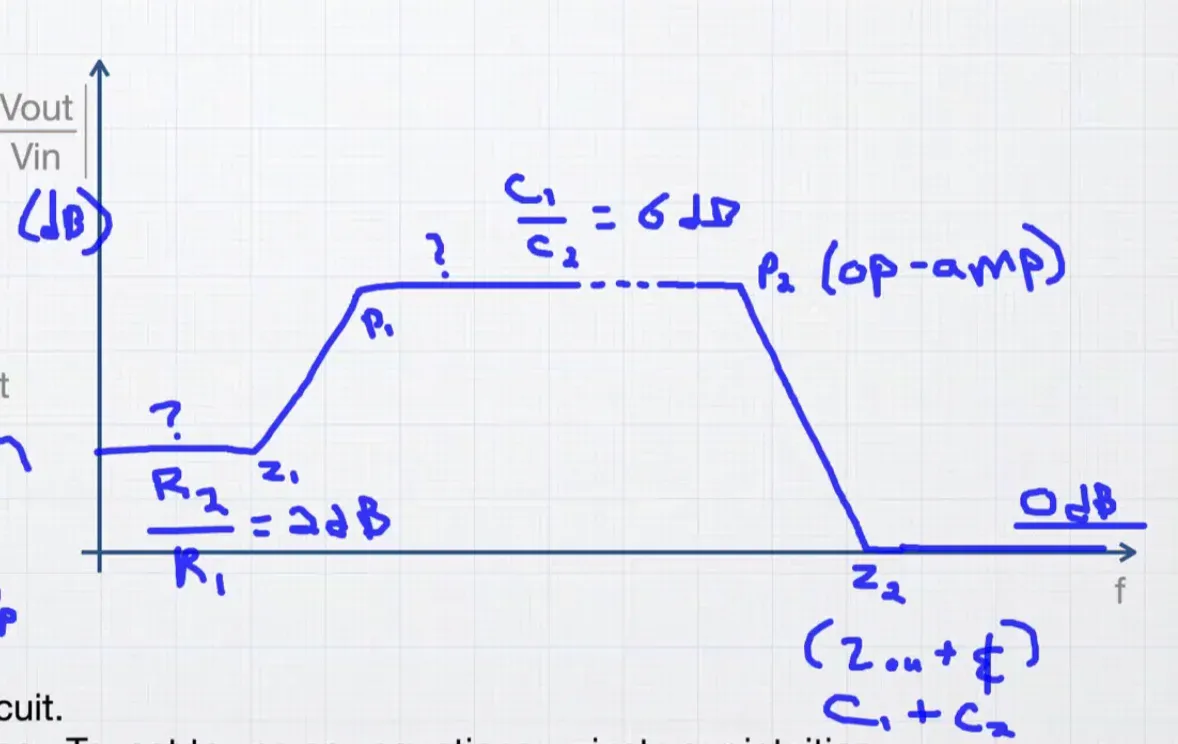
Bode Plot Walkthrough
| Frequency | What's Happening | Gain |
|---|---|---|
| Low | Caps open → resistors dominate | R₂/R₁ |
| Mid | Caps short → capacitors dominate | C₁/C₂ |
| High | Op-amp runs out of gain, rolls off | Dropping |
| Very High | Everything is shorted, passive divider | ~0 dB |
Key Answers
Both caps are shorts. Op-amp can't keep up. Circuit becomes a passive network → gain flattens near 0 dB.
The op-amp's open-loop gain is falling. When it can no longer enforce the virtual ground, the rolloff stops and a zero appears. It's the op-amp GBW interacting with the feedback network.
The peaking region (C₁/C₂) amplifies noise. Higher mid-band gain = worse noise performance.
Physical Design
Physical Design Fundamentals
Study Resources & Leetcode Numbers
🌐 Online Resources we use
- EDA Playground
Online Verilog/SystemVerilog simulator - montychoy.com
Ultimate list of hardware engineering internship interview questions - HDLBits
Leetcode but RTL Ver.1 - I personally like this one better - Chipdev
Leetcode but RTL Ver.2 - srnvl/Embedded_SWE_Prep
Embedded SWE Prep Github Repository - FIFO Depth Calculation Made Easy (PDF)
FIFO depth calculation guide - RFIC Interview Questions
RFIC interview questions - Asynchronous FIFO Verilog Code
Asynchronous FIFO Verilog Code - RTL Design Practice Problems
More RTL Interview Questions - UVM CookBook
Siemens Verification Academy UVM CookBook - Verification Guide (UVM TestBench architecture)
Coding UVM components - FSM-Finite State Machine-Questions
Some challenging FSM Questions - VLSI and hardware engineering interview questions
A painstakingly long question list (worth skimming through, there are few interesting questions) - DV Interview Prep Guide
Github repository for DV Interview Prep Guide - Example Interview Questions for a job in FPGA, VHDL, Verilog
From nandland youtube channel - Chipverify
Good resource for SystemVerilog/UVM/Verification - XOR Trick
XOR Trick that is good to know for interviews - Electronics Interview Questions: STA part 1
The typical STA interview question - Electronics Interview Questions: STA part 2
The 2nd typical STA interview question - What is AXI
Dillon Huff - Good Youtube channel for AXI protocol basics - Quick Review of Computer Architecture
Good Youtube channel for Computer Architecture for quick review of concepts - VLSI Verify
Verilog Interview Questions - Technical Internship Interview Questions
More interview questions - Computer Architecture Youtube Playlist
High Performance Computer Architecture (Udacity) - Ultimate Folder
Misc. list of VLSI interview questions
🔢 Leetcode Numbers
Most commonly asked LeetCode problems for Hardware Interview.
Embedded/Firmware Tips
We recommend using C and Python to solve these LeetCode questions. If you have to choose only one language, use C.